

Circuits for intrachip communications and networks-on-chip
 Using full-rail interfaces on chip (in which CMOS inverters drive CMOS over RC-dominated interconnect) is a very energy inefficient means of communication (for a given amount of bandwidth density) and results in unnecessarily long wire latencies. We have been developing techniques to take full advantage of the transmission line properties of on-chip wires to achieve high-bandwidth, low-latency, and low-energy on-chip interconnects. One testchip, shown below, uses distributed shunt negative conductance elements to compensate for transmission line losses in a 14-mm long link.
Related Publications
A. P. Jose and K. L. Shepard, “Distributed loss-compensation techniques for energy-efficient low-latency on-chip communications” IEEE Journal of Solid-State Circuits, Vol. 42, June, 2007, pp. 1415-1424.
Abstract
In this paper, we describe the use of distributed loss compensation to provide nearly transmission-line behavior for long on-chip interconnects. Negative impedance converters (NICs) inserted at regular intervals along an on-chip line are shown to reduce losses from more than 1 dB/mm to less than 0.3 dB/mm at 10 GHz. Results are presented for a 14-mm 3-Gb/s on-chip double-data-rate (DDR) link in 0.18- m CMOS technology, with a measured latency of 12.1 ps/mm and an energy consumption of less than 2 pJ/b with a BER 10 14. This constitutes a factor-of-three improvement in power and a one-and-a-half-times improvement in latency over an optimally repeated RC line of the same wire width.
A. P. Jose, G. Patounakis, and K. L. Shepard, “Pulse current-mode signalling for nearly speed-of-light intrachip communications” IEEE Journal of Solid-State Circuits, Vol. 41, April, 2006, pp. 772-780.
Abstract
In this paper, we describe the design of on-chip repeater-less interconnects with nearly speed-of-light latency. Sharp current-pulse data transmission is used to modulate transmitter energy to higher frequencies, where the effect of wire inductance is maximized, allowing the on-chip wires to function as transmission lines with considerably reduced dispersion. A prototype 8-Gb/s serial link employing this pulsed current-mode signaling in a 0.18- m CMOS process is described and measured.
A. P. Jose and K. L. Shepard, “Distributed loss compensation for low-latency on-chip interconnects” Digest of Technical Papers, International Solid-State Circuits Conference, 2006.
Continue reading →A. P. Jose, G. Patounakis, and K. L. Shepard, “Near speed-of-light on-chip interconnects using pulsed current-mode signalling” Symposium on VLSI Circuits, 2005.
Continue reading →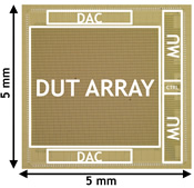
Measurement and modelling of variability in nanometer-scale CMOS
 Process variability is a critical concern in nanometer-scale CMOS, owing to random device fluctuations (dopant fluctuation, line-edge roughness) and also reticle and proximity effects, which have difficult-to-predict impacts on device characteristics. Traditionally, process variability is characterized by one of two methods: either individual devices with pads are characterized on an automated wafer stepper or a ‘silicon dense’ structure of ring oscillators is used to find correlations between frequency and variation. The first method provides high accuracy at the cost of large area overhead and low information throughput. The second method, although providing higher throughput, ‘integrates’ all the characteristics of multiple devices into one measured number dramatically reducing information content
 Recent methods focus on multiplexed transistor arrays because they provide high-density access to multiple devices for characterization. In our work, we have been designing on-chip current-voltage (I-V) measurement circuits that allow for rapid characterization of a large, dense array of multiplexed devices, using a four-point Kelvin-measurement approach to eliminate the effects of switch resistances and allowing for current measurements with nA resolution. Additionally, we have developed a novel, gate-leakage-insensitive on-chip charge-based capacitance measurement (CBCM) technique for capacitance-voltage (C-V)

characterization with aF resolution. Our CBCM technique enables us to characterize individual devices with circuit-representative dimensions in 45-nm CMOS, while at the same time largely reusing the on-chip measurement infrastructure already available for I-V characterization. More importantly, our combined C-V/I-V characterization approach allows us to not only study the variability in both sets of characteristics at the individual device level, but also to examine the correlation between them. As a result, by simultaneously observing and correlating the variability in the two measured sets of transistor characteristics, we are better able to infer the underlying physical causes of device variability.
Random telegraph noise (RTN) has been another source of growing concern in modern deep-sub-micron CMOS technologies. RTN is caused by the trapping and de-trapping of individual charges near the MOS transistor channel-oxide interface, resulting in telegraph-like modulation of the transistor current, and is expected to increase in magnitude with reduction of device size, eventually overtaking other traditional sources of device variability, such as random dopant fluctuations.  Our on-chip I-V characterization approach is ideally suited for RTN characterization, as it allows relatively high-frequency (up to 100 KHz) current measurements with nA resolution on large statistical device sets. In our work, we have measured RTN noise in a low-power 45-nm process, and we have developed a characterization and statistical modeling methodology that allows us to capture the effects of RTN on transistor performance.
Related Publications
S. Realov and K. L. Shepard, “On-Chip Combined C-V/I-V Transistor Characterization System in 45-nm CMOS,” Symposium on VLSI Circuits, 2011.
Abstract
An on-chip transistor characterization system for combined C-V/I-V characterization is presented. Capacitance measurement uses a quasi-static charged-based measurement technique with atto-Farad resolution. Random and systematic variability in device I-V and C-V characteristics is studied. The random variability in intrinsic gate capacitance is shown to exhibit Pelgrom scaling. Correlation between I-V and C-V measurements is used to identify systematic channel-length variation gradients in a device array.
S. Realov and K. L. Shepard, “Random telegraph noise in 45-nm CMOS: analysis using an on-chip test and measurement system,” International Electron Devices Meeting, 2010, pp. 28.2.1-28.2.4.
Abstract
RTN measurements in 45-nm CMOS across device bias and geometry using an on-chip characterization system are reported. An automated methodology for extracting RTN levels, amplitude and dwell times is developed. Complex RTN magnitude is statistically modeled, and device size and bias parameter dependencies of the developed model are examined.
V. Wang and K. L. Shepard, “On-chip transistor characterisation arrays for variability analysis” Electronics Letters, Vol. 43, No. 15, July, 19, 2007.
Abstract
efficiently and accurately characterise large, dense arrays of transistors for variability studies is designed. The prototype macro is used to perform current–voltage characterisation of a 2.8 mm2, 1600- transistor array with digital interfaces.